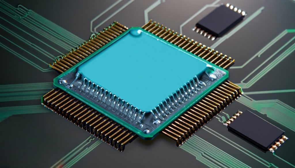
In the world of modern electronics, the Integrated Circuit (IC) stands as one of the most revolutionary inventions. An Integrated Circuit, commonly referred to as an IC or microchip, is a miniature electronic device that has the capability to perform a multitude of functions within a compact package. It has transformed the landscape of technology by enabling the creation of highly sophisticated and powerful electronic systems that are now integral to our daily lives.
At its core, an Integrated Circuit is a complex assembly of various electronic components such as transistors, resistors, capacitors, and diodes, meticulously embedded onto a tiny semiconductor wafer, usually made of silicon. These components are interconnected through intricate pathways, allowing them to work together cohesively. The magic lies in the miniaturization and integration of these components, which has led to the development of increasingly powerful and efficient electronic devices.
The inception of Integrated Circuits can be traced back to the mid-20th century when researchers like Jack Kilby and Robert Noyce made groundbreaking strides. Kilby’s invention of the first integrated circuit using germanium in 1958 and Noyce’s independent development of a silicon-based integrated circuit shortly after laid the foundation for the modern IC industry. These early ICs contained only a few components compared to the billions that today’s advanced microchips can accommodate.
Integrated Circuits come in various forms, ranging from simple analog circuits performing basic functions like amplification and signal processing, to complex digital circuits executing intricate tasks like data processing and control logic. The continuous advancement of semiconductor manufacturing technology has facilitated the creation of smaller transistors, enabling higher levels of integration and thus more powerful chips. This phenomenon is encapsulated in Moore’s Law, an observation made by Gordon Moore in 1965 that stated the number of transistors on a chip would double approximately every two years, leading to a consistent increase in computing power.
ICs have revolutionized industries such as computing, telecommunications, healthcare, and entertainment. They power our smartphones, laptops, medical devices, transportation systems, and much more. The compact size, efficiency, and reliability of ICs have not only made devices smaller and more portable but also more energy-efficient and cost-effective.
Types of Integrated Circuits
Integrated Circuits (ICs) come in a variety of types, each designed to serve specific functions and cater to various applications. These types of ICs can be broadly categorized into several main classes based on their functionality, complexity, and purpose. Here are some of the most common types of Integrated Circuits:
- Analog ICs: Analog ICs deal with continuous signals and are used for tasks like amplification, filtering, voltage regulation, and signal processing. Operational amplifiers (op-amps), voltage regulators, and analog-to-digital converters (ADCs) are examples of analog ICs. These ICs are crucial for tasks requiring accurate representation and manipulation of real-world signals.
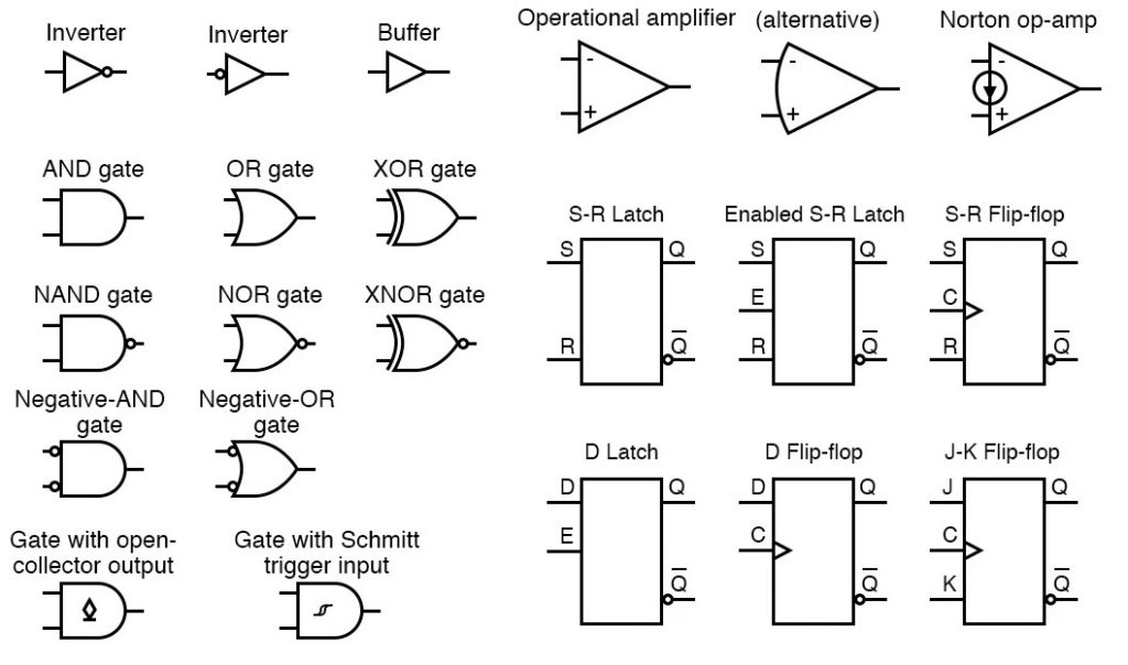
- Digital ICs: Digital ICs process discrete signals that have only two possible values: 0 and 1. They form the basis of digital logic and are used in applications like microprocessors, microcontrollers, digital signal processors (DSPs), and field-programmable gate arrays (FPGAs). Digital ICs are responsible for tasks such as computation, data storage, and logical operations.
- Microcontrollers: Microcontrollers (MCUs) are compact integrated circuits that combine a microprocessor core with memory and peripheral interfaces. They are the brains behind various embedded systems and control a wide range of devices, from household appliances to automotive systems.
- Microprocessors: Microprocessors are the heart of computing devices like computers and smartphones. They execute complex instructions, manage memory, and facilitate communication between different components of a system. Modern microprocessors are incredibly powerful and can execute billions of instructions per second.
- Memory ICs: These ICs are responsible for storing data in various forms. Types of memory ICs include:
- RAM (Random Access Memory): Provides temporary data storage for active processes.
- ROM (Read-Only Memory): Contains permanent instructions or data that cannot be modified.
- Flash Memory: Used for non-volatile data storage, often found in USB drives, memory cards, and solid-state drives (SSDs).
- Digital Signal Processors (DSPs): DSP ICs specialize in processing digital signals in real-time. They are used in applications such as audio processing, image processing, telecommunications, and control systems.
- Application-Specific Integrated Circuits (ASICs): ASICs are custom-designed ICs created for a specific application. They can be highly optimized for their intended purpose, offering improved performance and energy efficiency. ASICs are commonly used in specialized tasks where general-purpose ICs might not be as efficient.
- Field-Programmable Gate Arrays (FPGAs): FPGAs are unique ICs that can be reconfigured after manufacturing. They offer flexibility in implementing custom digital logic circuits and are often used in prototyping, research, and applications requiring rapid design iterations.
- Radio-Frequency ICs (RFICs): RFICs are designed to work in the radio frequency range, typically for wireless communication systems. They are used in devices like cell phones, Wi-Fi routers, and satellite communication systems.
- Power Management ICs: These ICs handle tasks related to power distribution, voltage regulation, and energy efficiency. They are essential components in electronic devices to ensure stable and efficient power delivery.
- Sensor ICs: Sensor ICs integrate sensors like accelerometers, gyroscopes, temperature sensors, and more. They are crucial for capturing real-world data and enabling devices to interact with their environment.
- Mixed-Signal ICs: These ICs combine both analog and digital components, making them suitable for applications that require processing both continuous and discrete signals. They are commonly found in systems where analog sensors feed data to digital processors.
These are just some of the many types of Integrated Circuits that play a fundamental role in modern electronics. The diversity and versatility of ICs enable the creation of an incredibly wide range of electronic devices, from the smallest wearables to the most powerful supercomputers.
Fabrication Process of Integrated Circuits
The fabrication process of Integrated Circuits (ICs) is a complex and highly precise sequence of steps that transforms a silicon wafer into a functional electronic device containing numerous transistors, resistors, capacitors, and interconnections. This process involves a combination of photolithography, etching, doping, deposition, and other techniques. Here’s an overview of the typical fabrication process of ICs:
- Wafer Preparation: The process begins with the preparation of a silicon wafer. The silicon wafer is a thin, circular disk that serves as the substrate for the ICs. The wafer is first cleaned to remove any contaminants or impurities.
- Oxidation: A thin layer of silicon dioxide (SiO2) is grown on the surface of the silicon wafer through a process called thermal oxidation. This oxide layer serves as an insulator and provides isolation between different components.
- Photolithography:
- Photoresist Coating: A layer of photoresist, a light-sensitive material, is applied to the wafer’s surface.
- Mask Alignment: A mask, which is a patterned template, is aligned over the wafer. The mask defines the pattern of features that will be created on the wafer.
- Exposure: Ultraviolet (UV) light is shone through the mask onto the photoresist-coated wafer. The exposed photoresist becomes either more soluble (positive resist) or less soluble (negative resist) depending on the type of resist used.
- Etching:
- Developing: The wafer is immersed in a chemical solution to remove the exposed (developed) areas of photoresist, revealing the underlying silicon dioxide layer.
- Etch: The exposed silicon dioxide is etched away using chemicals. This step transfers the mask pattern onto the silicon dioxide layer.
- Doping:
- Ion Implantation: Dopants, which are atoms that alter the electrical properties of silicon, are implanted into the wafer using ion implantation. This step introduces regions of n-type (electron-rich) and p-type (hole-rich) silicon, forming transistors and other components.
- Deposition:
- Thin-Film Deposition: Thin films of materials such as metals (like aluminum) or dielectrics (like silicon nitride) are deposited onto the wafer’s surface using techniques like chemical vapor deposition (CVD) or physical vapor deposition (PVD).
- Additional Photolithography and Etching: Additional photolithography and etching steps are performed to define and create various layers of transistors, interconnects, and other components. This multi-layer process allows for the creation of complex structures.
- Planarization: To ensure a flat surface for subsequent layers, planarization techniques like chemical-mechanical polishing (CMP) may be employed. This step helps maintain uniformity across the wafer’s surface.
- Contact and Via Formation: Openings called contacts and vias are etched to allow electrical connections between different layers. Metal is then deposited into these openings to create the interconnections.
- Insulating Layer Deposition: Additional insulating layers are deposited to isolate and protect the interconnections.
- Back-End-of-Line (BEOL) Processing: The final stages of IC fabrication involve creating the top metal layers and completing the interconnections between different components.
- Testing and Packaging: Once the fabrication process is complete, the wafer is subjected to rigorous testing to identify any defects or malfunctions. After testing, the wafer is diced into individual chips, and each chip is packaged in a protective casing that provides electrical connections to the outside world.
The fabrication process of Integrated Circuits is a meticulous and intricate endeavor that requires advanced technology, precision equipment, and expertise. Over the years, advancements in semiconductor manufacturing have led to the creation of smaller transistors, allowing for increased levels of integration and improved performance in electronic devices.
IC Design Methodology
Integrated Circuit (IC) design methodology encompasses the systematic and organized approach to creating complex electronic circuits that are integrated onto a single chip. This process involves a series of steps that ensure the successful development of functional and efficient ICs. Here is an overview of the typical IC design methodology:
- Specification and Requirement Analysis:
- The design process begins with understanding the requirements and specifications of the desired IC. This includes defining its functionality, performance targets, power consumption limits, and other key parameters.
- Clear communication between designers and stakeholders is crucial to establish a common understanding of the project’s goals.
- Architecture Design:
- The high-level architecture of the IC is planned during this phase. Designers determine the overall structure, including major blocks, interfaces, and data flow.
- Key decisions regarding the choice of analog or digital components, memory, and communication protocols are made at this stage.
- Functional Design and Modeling:
- Designers create detailed functional models of each block or module within the IC.
- Modeling techniques like hardware description languages (HDLs) such as Verilog or VHDL are used to describe the behavior and interactions of different components.
- Logic Design:
- In the logic design phase, designers convert the functional models into digital logic circuits.
- This involves specifying gate-level logic, creating digital components (adders, multiplexers, flip-flops), and defining control logic.
- Circuit Design:
- At the circuit level, designers create detailed schematics of individual components using transistors and other basic electronic elements.
- Analog components like amplifiers, filters, and voltage regulators are designed during this phase.
- Verification and Simulation:
- Before moving to physical implementation, extensive simulation is performed to validate the design’s functionality, timing, and performance.
- Simulation tools allow designers to catch errors and make necessary optimizations in a virtual environment.
- Physical Design:
- Physical design involves translating the logical and circuit-level designs into the actual layout on the silicon wafer.
- It includes floor planning, placement, routing, and timing optimization to ensure that signals propagate correctly and efficiently.
- Design for Manufacturability (DFM) and Design for Testability (DFT):
- DFM aims to optimize the design for the manufacturing process, considering factors like lithography limitations, process variability, and yield enhancement.
- DFT techniques are incorporated to ensure that the final IC can be effectively tested during manufacturing to identify defects.
- Mask Generation:
- Based on the final layout, a set of masks is generated. These masks guide the fabrication process by defining the patterns to be etched onto the silicon wafer.
- Fabrication and Manufacturing:
- The masks are used in the semiconductor fabrication process to create the actual ICs on silicon wafers through techniques such as photolithography and doping.
- Testing and Debugging:
- Once manufactured, the ICs undergo rigorous testing to identify defects and ensure they meet the specified performance criteria.
- Debugging and analysis tools are employed to diagnose any issues that arise during testing.
- Packaging and Final Testing:
- The tested ICs are packaged to protect them and provide electrical connections for external use.
- Final testing is conducted to verify the IC’s functionality in its packaged form.
IC design methodology is an iterative process, often involving multiple cycles of design, simulation, testing, and refinement. It requires interdisciplinary collaboration, incorporating aspects of electrical engineering, physics, materials science, and computer science. Advancements in design tools and methodologies have been instrumental in creating increasingly complex and efficient ICs that power a wide range of electronic devices.
Scaling of Integrated Circuits
Scaling in the context of Integrated Circuits (ICs) refers to the reduction in the size of individual transistors and other components on a semiconductor chip while simultaneously increasing the number of components that can be integrated onto that chip. The concept is central to Moore’s Law, which observes that the number of transistors on a chip roughly doubles every two years, leading to improvements in performance, energy efficiency, and cost per transistor.
Here’s an overview of the significance and implications of scaling in ICs:
1. Miniaturization:
- Scaling involves shrinking the size of transistors and interconnects on a chip. As components become smaller, the distance that signals need to travel within the chip decreases, leading to faster operation and reduced power consumption.
2. Increased Integration:
- Smaller components allow for more components to be packed onto a single chip. This increased integration leads to the creation of more complex and powerful ICs, enabling advanced functionalities.
3. Performance Improvements:
- Smaller transistors can switch on and off more quickly, leading to higher clock speeds and improved processing capabilities. This results in better overall performance for electronic devices.
4. Energy Efficiency:
- Smaller transistors require less energy to switch on and off, leading to improved energy efficiency. Devices built with smaller transistors consume less power, which is particularly important for battery-operated devices.
5. Cost Reduction:
- As the number of transistors on a chip increases with scaling, the cost per transistor typically decreases. This has historically contributed to making electronic devices more affordable over time.
6. Challenges and Innovations:
- Scaling also presents challenges, including quantum effects, leakage currents, and manufacturing complexities. To continue scaling, innovations in materials, transistor structures (like FinFETs), and manufacturing processes (like extreme ultraviolet lithography) have been developed.
7. Limits of Scaling:
- As components approach atomic scales, they are susceptible to quantum mechanical effects, making it challenging to maintain traditional behavior. Heat dissipation and leakage currents also become more problematic as components shrink.
- The industry has explored alternative technologies like 3D stacking (integrating multiple layers of chips) and novel materials (like graphene) to extend scaling beyond traditional limits.
8. Beyond Moore’s Law:
- While Moore’s Law has driven the semiconductor industry for decades, it’s important to note that the rate of transistor density increase has slowed in recent years. This has led to a shift from relying solely on transistor scaling to exploring system-level optimizations, specialized architectures, and new computing paradigms.
Scaling is a foundational principle of IC design that has enabled the development of increasingly powerful and compact electronic devices. It has shaped the evolution of technology and transformed various industries. While challenges exist in pushing traditional scaling further, ongoing innovations continue to drive advancements in semiconductor manufacturing and design.
Conclusion
Integrated Circuits (ICs) stand as one of the most transformative inventions in the realm of electronics. These miniature marvels, crafted through intricate processes, have redefined the boundaries of technological progress and shaped the modern world in profound ways. From the foundational work of early pioneers to the cutting-edge advancements of today, ICs have revolutionized industries, empowered innovation, and become integral to nearly every facet of our lives.
The journey from the humble beginnings of the first ICs to the sophisticated microchips of today reflects not only the prowess of human ingenuity but also the relentless pursuit of efficiency, performance, and miniaturization. The art and science of IC design and fabrication have merged to create devices that are not only immensely powerful but also energy-efficient, affordable, and capable of fitting inconceivable complexity onto a fingernail-sized chip.
The types of ICs have diversified, from analog to digital, from microcontrollers to memory chips, each tailored to meet specific needs across a spectrum of applications. The methodical IC design process, from specification to manufacturing, has become a symphony of creativity, engineering precision, and multidisciplinary collaboration. Scaling, a fundamental principle in IC design, has enabled us to witness the ever-accelerating pace of technological advancement, reshaping the way we communicate, compute, and interact with the world.
As we venture into the future, the potential of ICs remains boundless. With advancements in AI, quantum computing, and emerging technologies, we are on the cusp of a new era where the capabilities of Integrated Circuits will undoubtedly push the boundaries of what we thought was possible. ICs will continue to empower innovation, drive economic growth, and shape the landscape of our interconnected world.
In essence, Integrated Circuits encapsulate human creativity, scientific progress, and the relentless pursuit of efficiency within their intricate pathways and minuscule components. They have transcended the realm of mere electronic components to become the building blocks of our digital civilization. As we move forward, the story of ICs will continue to unfold, inspiring generations of engineers, scientists, and visionaries to harness their potential and propel us towards uncharted technological horizons.